Top level Diagram
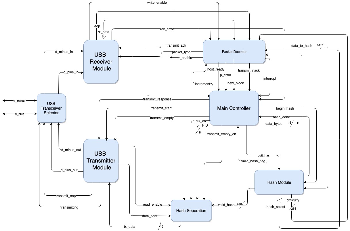
Here is the top level architecture block diagram for the whole miner. It includes 5 major components. USB Receiver, USB Transmitter, Packet Decoder, Hash Module, and the Main Controller.
Here is some of the documentation for our class project where we designed an ASIC hardware accelerator that would mine bitcoin for you with a simple USB interface. I worked on this project with 3 other teammates, Rahul Patni, Yash Bharatula and Chinar Dhamija. The documentation here is sparse as I am not interested in rewriting it all. If you are interested, you can read the full report here.
Here is the top level architecture block diagram for the whole miner. It includes 5 major components. USB Receiver, USB Transmitter, Packet Decoder, Hash Module, and the Main Controller.
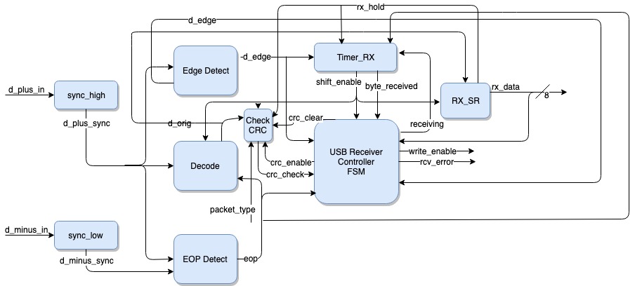
Here is the block diagram for the USB Receiver. It decodes the USB packets to groups of bytes and sends them along to the packet decoder/ main state machine. It also does some sanity checking by checking that the packets were meant to be sent to this device and the CRC checksum is correct on each packet.
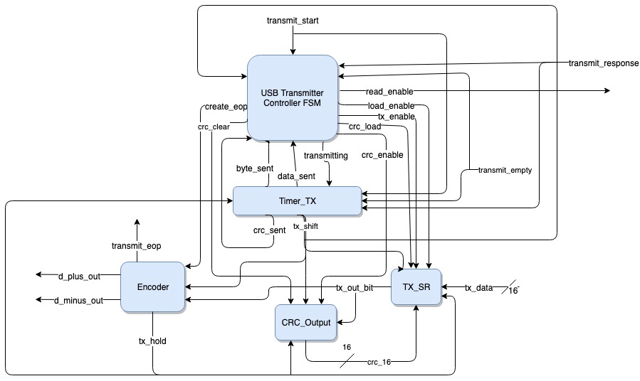
Here is the top level architecture block diagram for the USB transmitter. It receives starting signals from the main controller to output data packets and transmits ACK, and DATA packets at the appropriate times and with the correct USB 1.1 protocol.
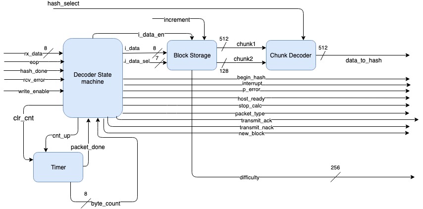
This is the packet decoder block diagram. This module is given full USB packets and makes decisions based on the type of packet it receives. It also has a small memory storage called Block Storage that stores the block to be hashed as it comes in.
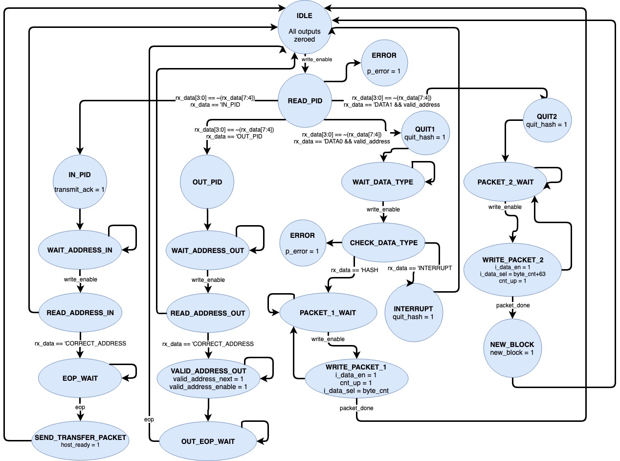
Here is the state machine at the heart of the packet decoder. There are 4 main paths, it can take based on the initial PID packet. IN, OUT, DATA0 or DATA1. IN means that new data is coming into the miner. OUT is where the master is requesting data out of the miner. If the miner has found a successful hash then it will return data if not it will reply stating that nothing has been found. The last 2 types, DATA0 and DATA1 are the bitcoin input block data payload.
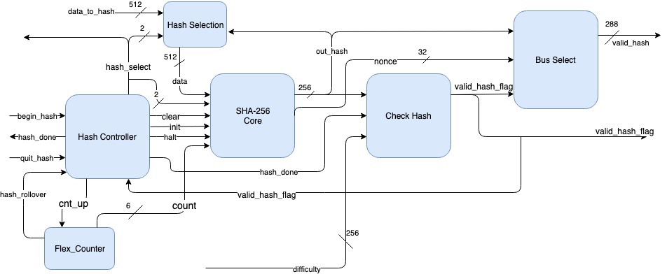
Here is the block diagram for the hash module. It is started from the main controller and has a little state machine that sends correct control signals to the SHA_256 blocks. It takes 64 clock cycles to calculate one SHA-256 hash. After that the hash is checked to see if that block has enough leading zeros to ensure the proof of work. If that is incorrect the nonce is incremented and we try again.
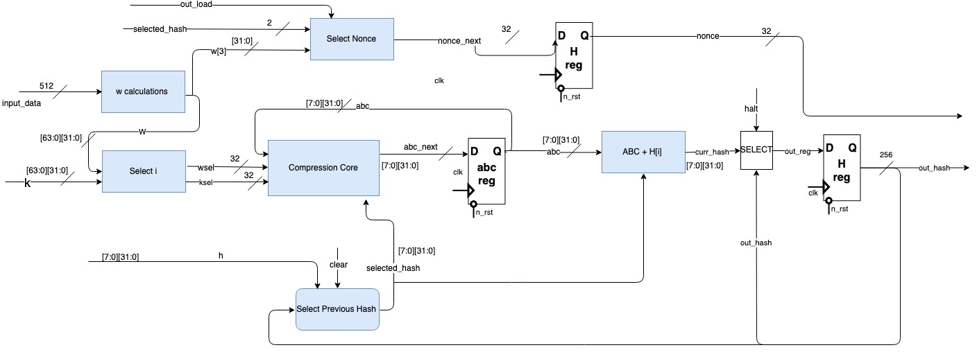
This is how the SHA-256 core functions in hardware. To really understand this one would need to read the documentation on how SHA-2 works.
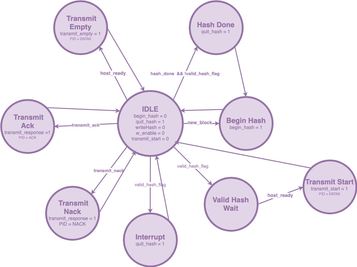
Lastly we have the main controller. It is a relatively simple state machine. Initally we had this block doing a lot of the heavy lifting in terms of packet decoding but it made more sense as we moved along to put state machines in both the packet decoder and Hash module. This made the workload for this block pretty light. Overall it is kicked on by new packets from the USB_RX and the packet decoder and moves control signals around to the various modules.
Overall this project was really challenging and pushed us to work quickly and think deeply on how data is moved around in real world systems. In the end the most challenging aspect of the design was getting the USB modules to work well. We thought it would be easy to just 'insert' usb modules but it was so much more work. The timing and ordering of the data was very complex. I'm glad we worked on this and im glad I learned a lot on how to test work together on a design in a team.